X-Ray Diffraction (XRD) Foundation Course
Prerequisites: Basic understanding of unit cells and lattice parameters recommended but not required
Reading time: 45 minutes | Includes: Interactive Bragg's Law calculator, crystal structure visualization, Miller indices decoder, XRD pattern interpretation guide, worked examples, practice questions, key takeaways
SEO Keywords: X-ray diffraction tutorial, Bragg's law explained, 2theta vs theta XRD, Miller indices made simple, XRD pattern interpretation, crystal structure determination, materials characterization
Pain Points Addressed: "I don't understand Bragg's Law" | "What's the difference between θ and 2θ?" | "Miller indices are confusing" | "What information is in each XRD peak?"
- What is X-Ray Diffraction?
- The Story Behind XRD: Nobel Prize Discovery
- Bragg's Law Explained — Visual Step-by-Step
- Understanding 2θ vs θ — The Most Common Confusion
- Crystal Structures Basics (FCC, BCC, HCP)
- Miller Indices Made Simple
- What Does an XRD Pattern Actually Tell You?
- Peak Position, Intensity, and Width — What They Mean
- Worked Examples
- Practice Questions
- Key Takeaways
- References
1. What is X-Ray Diffraction?
Imagine you are a detective trying to identify an unknown crystalline material. You cannot see individual atoms — they are far too small for any optical microscope. But you need to know: What is its crystal structure? How are the atoms arranged? What are the lattice parameters? Is it pure, or does it contain impurities?
This is where X-ray diffraction (XRD) becomes your most powerful investigative tool. XRD is a non-destructive analytical technique that reveals the atomic and molecular structure of crystalline materials by measuring the angles and intensities at which X-rays are scattered (diffracted) by the crystal lattice.
1.1 Real-World Applications
XRD is not confined to university laboratories — it is an indispensable tool across multiple industries and research fields:
Pharmaceutical Industry: Ensuring that active pharmaceutical ingredients (APIs) crystallize in the correct polymorphic form. For example, different crystal forms of the same drug molecule can have drastically different solubility and bioavailability. XRD is used to verify the correct polymorph during drug development and quality control.
Semiconductor Manufacturing: Silicon wafers, gallium nitride (GaN) LEDs, and III-V compound semiconductors require precise crystal orientation and minimal defects. XRD verifies crystal quality, epitaxial layer thickness, and strain in thin films.
Materials Engineering: Identifying phases in steel alloys, determining the degree of crystallinity in polymers, analyzing residual stress in machined components, and studying phase transformations in functional materials like shape-memory alloys.
Geology and Mineralogy: Identifying mineral compositions in rock samples, studying clay minerals in soil science, and analyzing meteorite samples to understand planetary formation.
Forensic Science: Analyzing crystalline materials in evidence samples — from explosives residues to counterfeit pharmaceutical tablets.
Battery Research: Characterizing the crystal structure of cathode and anode materials in lithium-ion batteries. Structural changes during charge-discharge cycles can be monitored in real-time using in-situ XRD.
1.2 Why XRD is the Gold Standard
Among all materials characterization techniques, XRD stands out because it provides direct, unambiguous structural information. Unlike electron microscopy (which images surfaces), spectroscopy (which probes chemical composition), or calorimetry (which measures thermal properties), XRD tells you exactly how atoms are arranged in three-dimensional space.
The power of XRD lies in three fundamental advantages:
- Non-destructive: The sample remains intact after measurement. You can analyze the same sample multiple times or use it for further experiments.
- Quantitative: XRD provides precise numerical data — lattice parameters accurate to four decimal places, phase fractions in mixtures, crystallite sizes from nanometers to micrometers.
- Universal: Every crystalline material has a unique XRD "fingerprint" — its diffraction pattern. This fingerprint can be compared against databases containing hundreds of thousands of known structures.
2. The Story Behind XRD: Nobel Prize Discovery
The story of X-ray diffraction is a tale of scientific serendipity, father-son collaboration, and one of the youngest Nobel Prize winners in history.
2.1 Röntgen's Discovery (1895)
It began in 1895 when German physicist Wilhelm Röntgen discovered X-rays while experimenting with cathode ray tubes. He noticed that a fluorescent screen across the room glowed whenever the tube was operating — even when shielded with black cardboard. Röntgen had discovered a new form of penetrating radiation, which he called "X-rays" (X for unknown). He won the first-ever Nobel Prize in Physics in 1901.
But Röntgen did not understand the true nature of X-rays. Were they particles? Waves? The answer would come 17 years later.
2.2 Von Laue's Breakthrough (1912)
In 1912, German physicist Max von Laue hypothesized that if X-rays were waves with wavelengths comparable to atomic spacing (~0.1–1 nm), then crystals — with their regular, periodic atomic arrangements — should act as three-dimensional diffraction gratings. He predicted that X-rays passing through a crystal would produce a characteristic diffraction pattern.
His assistants Walter Friedrich and Paul Knipping tested the hypothesis by directing X-rays through a copper sulfate crystal. The photographic plate behind the crystal revealed a stunning pattern of spots — the world's first X-ray diffraction pattern. This proved two things simultaneously: X-rays are electromagnetic waves, and crystals have a periodic atomic structure. Von Laue won the Nobel Prize in Physics in 1914.
2.3 The Braggs' Equation (1912–1913)
Just months after von Laue's discovery, British physicist William Henry Bragg and his 22-year-old son William Lawrence Bragg developed a simpler, more practical explanation of X-ray diffraction. Rather than treating it as a complex three-dimensional diffraction problem, they modeled it as reflection from parallel planes of atoms within the crystal.
The younger Bragg derived the elegant equation that now bears their name:
This single equation revolutionized crystallography. The Braggs used it to determine the crystal structures of sodium chloride (NaCl), diamond, and many other materials — the first-ever direct determination of atomic arrangements. Their groundbreaking work laid the foundation for modern structural biology, materials science, and solid-state physics. You can read more about their discovery and its impact on the official Nobel Prize website, which provides detailed historical context and the original Nobel lecture transcripts.
The development of XRD marks one of the great intellectual achievements of the 20th century. It opened the door to understanding matter at the atomic level — from the double helix of DNA (determined by Rosalind Franklin using XRD) to the structure of proteins, semiconductors, and functional nanomaterials.
3. Bragg's Law Explained — Visual Step-by-Step
Bragg's Law is the foundation of X-ray diffraction. Once you understand it deeply, interpreting XRD patterns becomes straightforward. Let us build the concept step by step, starting from first principles.
3.1 The Analogy: Skipping Stones on Water
Imagine skipping a stone across a calm lake. The stone bounces off the water surface at the same angle it came in — the angle of incidence equals the angle of reflection. This is exactly how we model X-ray diffraction in the Bragg approach: X-rays "reflect" from parallel planes of atoms inside the crystal.
But there is a critical difference: in a crystal, there are many parallel atomic planes, stacked one behind the other. X-rays reflect not just from the top plane, but from every plane beneath it. For these reflected waves to constructively interfere and produce a detectable diffraction peak, they must arrive at the detector in phase — meaning their wave crests align perfectly.
3.2 Derivation of Bragg's Law
Consider two parallel atomic planes separated by a distance d (the interplanar spacing). An incoming X-ray beam strikes these planes at an angle θ (measured from the plane surface, not the normal — this is important!).
The X-ray reflected from the second plane travels an extra distance compared to the ray reflected from the first plane. This extra distance is called the path difference.
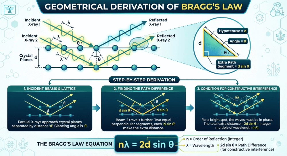
Fig. 1: Geometric derivation of Bragg's Law. Two parallel atomic planes separated by distance d. The X-ray beam reflected from the lower plane travels an extra distance (path difference = 2d sinθ). For constructive interference, this path difference must equal nλ. | Recommended source: IUCr Educational Pamphlets
Geometric analysis shows that the path difference is:
For constructive interference (a bright diffraction spot), this path difference must equal an integer number of wavelengths:
Where:
- n = order of diffraction (1, 2, 3, ...) — an integer representing the number of wavelengths in the path difference
- λ = wavelength of the X-ray beam (typically CuKα = 1.5406 Å, fixed and known)
- d = interplanar spacing (the distance between parallel atomic planes — this is what we want to measure)
- θ = Bragg angle (half of the diffraction angle 2θ measured by the detector)
4. Understanding 2θ vs θ — The Most Common Confusion
This confusion trips up nearly every student learning XRD for the first time. The distinction is simple once you visualize the experimental geometry.
4.1 The Experimental Geometry
In a typical powder XRD instrument (Bragg-Brentano geometry), the setup looks like this:
- The X-ray source is fixed in position
- The sample is mounted on a rotating stage
- The detector moves around the sample to collect diffracted X-rays
As the sample rotates by an angle θ, the detector must rotate by 2θ to intercept the diffracted beam. This is because of the reflection geometry: the diffracted beam makes the same angle θ with the sample surface as the incident beam, but on the opposite side.
- θ (theta) = the Bragg angle = the angle between the incident X-ray beam and the atomic planes = the angle used in Bragg's Law
- 2θ (two-theta) = the diffraction angle = the total angle between the incident beam direction and the detector position = what the instrument measures and what appears on the XRD pattern x-axis
4.2 Why XRD Patterns Use 2θ
XRD patterns always plot intensity (y-axis) versus 2θ (x-axis) because 2θ is what the detector physically measures. The detector angle is directly observable; the Bragg angle θ is a derived quantity.
When you see a diffraction peak at 2θ = 45°, it means:
- The detector is positioned at 45° from the incident beam direction
- The Bragg angle is θ = 45°/2 = 22.5°
- You use θ = 22.5° in Bragg's Law to calculate the d-spacing
Solution:
First, find the Bragg angle: θ = 38.5° / 2 = 19.25°
Then apply Bragg's Law (assuming first-order diffraction, n = 1):
d = λ / (2 sinθ) = 1.5406 / (2 × sin(19.25°)) = 1.5406 / (2 × 0.3297) = 2.336 Å
4.3 Quick Conversion Guide
| What You See on XRD Pattern | Bragg Angle (for calculation) | Used in Bragg's Law as: |
|---|---|---|
| 2θ = 20° | θ = 10° | d = λ / (2 sin(10°)) |
| 2θ = 40° | θ = 20° | d = λ / (2 sin(20°)) |
| 2θ = 60° | θ = 30° | d = λ / (2 sin(30°)) |
| 2θ = 80° | θ = 40° | d = λ / (2 sin(40°)) |
5. Crystal Structures Basics (FCC, BCC, HCP)
Before we can interpret XRD patterns, we need to understand what we're looking at: the crystal structures themselves. All crystalline materials belong to one of seven crystal systems, but three structures dominate engineering materials: Face-Centered Cubic (FCC), Body-Centered Cubic (BCC), and Hexagonal Close-Packed (HCP). For a foundational introduction to crystal structures and the concept of lattice plus basis, start with our crystal structure introduction tutorial.
5.1 Face-Centered Cubic (FCC)
Unit cell description: A cube with atoms at each of the eight corners AND at the center of each of the six faces. For a comprehensive deep-dive into the FCC structure including derivations of atomic radius, packing efficiency, and coordination number, see our detailed FCC crystal structure tutorial.
Atoms per unit cell: Using the sharing rule: 8 corners × (1/8) + 6 faces × (1/2) = 1 + 3 = 4 atoms
Coordination number: 12 (each atom touches 12 nearest neighbors — the maximum possible for identical spheres)
Packing efficiency: 74% — the highest achievable for identical spheres (also achieved by HCP)
Common examples: Copper (Cu), Aluminum (Al), Gold (Au), Silver (Ag), Nickel (Ni), Lead (Pb), Platinum (Pt)
Why it matters for XRD: FCC structures have systematic absences in their diffraction patterns. Not all (hkl) reflections appear — only those where h, k, l are all even or all odd. This is a consequence of destructive interference from the face-centered atoms.
5.2 Body-Centered Cubic (BCC)
Unit cell description: A cube with atoms at each of the eight corners AND one atom at the center of the cube. For detailed calculations including atomic packing factor, nearest neighbor distances, and worked examples, explore our complete BCC crystal structure tutorial.
Atoms per unit cell: 8 corners × (1/8) + 1 center × 1 = 2 atoms
Coordination number: 8 (each atom touches 8 nearest neighbors)
Packing efficiency: 68% — less dense than FCC
Common examples: Iron (Fe) at room temperature (α-Fe), Chromium (Cr), Tungsten (W), Molybdenum (Mo), Vanadium (V)
Why it matters for XRD: BCC structures also have systematic absences — only reflections where (h + k + l) is even will appear. The (100), (300), (111), (221) reflections are forbidden.
5.3 Hexagonal Close-Packed (HCP)
Unit cell description: A hexagonal prism with atoms at the corners and additional atoms in a specific stacking pattern (ABABAB...). To understand the c/a ratio, stacking sequences, and how HCP differs from FCC despite identical packing efficiency, read our in-depth HCP crystal structure tutorial.
Atoms per unit cell: 2 atoms (in the simplest representation)
Coordination number: 12 (same as FCC — both are close-packed structures)
Packing efficiency: 74% (identical to FCC, but with different stacking sequence)
Common examples: Magnesium (Mg), Zinc (Zn), Titanium (Ti), Cobalt (Co), Zirconium (Zr)
Why it matters for XRD: HCP requires two lattice parameters (a and c) instead of one. The c/a ratio determines the peak positions and can vary from material to material.
6. Miller Indices Made Simple
Miller indices are a notation system for labeling planes and directions in crystals. Every XRD peak corresponds to diffraction from a specific set of parallel atomic planes, and those planes are identified by their Miller indices (hkl). For a complete step-by-step guide with interactive visualizations and multiple worked examples, see our comprehensive Miller indices tutorial.
6.1 What Are Miller Indices?
Miller indices (hkl) are three integers that uniquely describe the orientation of a plane in the crystal lattice. They are NOT coordinates — they are derived from the intercepts that the plane makes with the crystallographic axes.
6.2 How to Determine Miller Indices — Step by Step
To find the Miller indices of a plane, follow this procedure:
- Find the intercepts: Determine where the plane intersects the x, y, and z axes (in terms of lattice constants a, b, c). If a plane is parallel to an axis, the intercept is at infinity (∞).
- Take reciprocals: Take the reciprocal of each intercept. The reciprocal of ∞ is 0.
- Clear fractions: Multiply all three reciprocals by the smallest number that converts them to integers.
- Write as (hkl): Enclose the three integers in parentheses. These are the Miller indices.
Solution:
1. Intercepts: 1, 2, 3
2. Reciprocals: 1/1, 1/2, 1/3
3. Clear fractions (multiply by 6): 6, 3, 2
4. Miller indices: (632)
6.3 Common Miller Indices in Cubic Crystals
Fig. 2: Visualization of common crystallographic planes in a cubic crystal: (100) plane cuts x-axis only, (110) plane cuts x and y axes, (111) plane cuts all three axes equally. Each plane family produces a distinct diffraction peak in XRD patterns. | Recommended source: DoITPoMS Miller Indices Tutorial (University of Cambridge)
| Miller Indices | Description | Intercepts (a, b, c) |
|---|---|---|
| (100) | Plane parallel to y-z axes, cuts x-axis at 1a | 1, ∞, ∞ |
| (010) | Plane parallel to x-z axes, cuts y-axis at 1b | ∞, 1, ∞ |
| (001) | Plane parallel to x-y axes, cuts z-axis at 1c | ∞, ∞, 1 |
| (110) | Plane cuts x at 1a, y at 1b, parallel to z | 1, 1, ∞ |
| (111) | Plane cuts all three axes at 1a, 1b, 1c | 1, 1, 1 |
| (200) | Plane cuts x at a/2, parallel to y and z | 1/2, ∞, ∞ |
6.4 Why Miller Indices Matter in XRD
Every diffraction peak in an XRD pattern corresponds to a specific (hkl) plane family. The (111) peak comes from the (111) planes, the (200) peak from the (200) planes, and so on. By identifying which peaks appear (and which are absent), you can:
- Determine the crystal structure (FCC, BCC, HCP, etc.)
- Calculate the lattice parameter using the relationship between d-spacing and (hkl)
- Identify the material by comparing the pattern to a database
6.5 The d-spacing Formula for Cubic Crystals
For cubic crystals (where a = b = c and all angles are 90°), the relationship between the d-spacing and Miller indices is particularly simple. For complete derivations and applications of this formula across all seven crystal systems, see our unit cell and lattice parameters tutorial.
This formula is extraordinarily useful. Once you know the lattice parameter a and the Miller indices (hkl), you can predict the exact position of every diffraction peak. Conversely, if you measure the d-spacing from an XRD peak, you can work backward to determine a.
7. What Does an XRD Pattern Actually Tell You?
An XRD pattern is a plot of diffraction intensity (y-axis) versus 2θ angle (x-axis). At first glance, it looks like a series of sharp peaks of varying heights at specific angles. But this seemingly simple graph contains a wealth of structural information.
7.1 Anatomy of an XRD Pattern
A typical powder XRD pattern consists of:
- Diffraction peaks: Sharp spikes that appear at specific 2θ values where Bragg's Law is satisfied
- Background: A low, broad baseline signal from air scattering, sample fluorescence, and instrumental noise
- Baseline: The zero-intensity reference level
Each diffraction peak encodes three pieces of information:
- Peak position (2θ value): Tells you the d-spacing of the diffracting planes via Bragg's Law
- Peak intensity (height or integrated area): Tells you how many atoms are in the diffracting planes and their scattering power
- Peak width (full width at half maximum, FWHM): Tells you the crystallite size and microstrain in the sample
7.2 The Fingerprint Concept
Every crystalline material has a unique XRD pattern — its structural "fingerprint." Two materials with different crystal structures will have different peak positions, intensities, and widths. This is why XRD is used for phase identification: you match your experimental pattern against a database of known patterns.
The largest and most comprehensive database is the Powder Diffraction File (PDF) maintained by the International Centre for Diffraction Data (ICDD). It contains over 1 million reference patterns. For educational resources and standardization guidelines on powder diffraction methods, the International Union of Crystallography (IUCr) provides authoritative technical documentation and best practices used by researchers worldwide.
2. Identify the peak positions (2θ values)
3. Calculate the d-spacings using Bragg's Law
4. Search the PDF database for materials with matching d-spacings
5. Compare the relative intensities to narrow down the candidates
6. Verify the match by checking that ALL peaks align
7.3 What You Can Learn from an XRD Pattern
| Information | How XRD Reveals It |
|---|---|
| Crystal structure type | Peak positions and systematic absences (FCC, BCC, HCP, etc.) |
| Lattice parameters (a, b, c) | Calculated from d-spacings and Miller indices |
| Phase identification | Matching pattern to reference database |
| Phase purity | Presence or absence of extra peaks from impurities |
| Phase composition (quantitative) | Rietveld refinement of relative peak intensities |
| Crystallite size | Peak broadening analysis (Scherrer equation) |
| Microstrain | Peak broadening and peak shift analysis |
| Preferred orientation (texture) | Deviation of peak intensities from random powder |
| Residual stress | Shifts in peak positions from lattice distortion |
8. Peak Position, Intensity, and Width — What They Mean
8.1 Peak Position — Structural Information
What it tells you: The 2θ position of a peak directly tells you the d-spacing of the diffracting planes through Bragg's Law.
Why it matters: Different materials have different d-spacings. Even a small shift in peak position (as little as 0.01° in 2θ) can indicate:
- A change in lattice parameter (from thermal expansion, doping, or alloying)
- Residual stress (compressive stress shifts peaks to higher 2θ, tensile stress to lower 2θ)
- Phase transformation (different crystal structures have different peak positions)
8.2 Peak Intensity — Atomic Arrangement
What it tells you: The intensity (height or integrated area) of a peak depends on:
- Structure factor: How many atoms are in the diffracting planes and what types of atoms they are (heavier atoms scatter X-rays more strongly)
- Multiplicity: How many equivalent plane orientations contribute to the same peak
- Lorentz-polarization factor: Geometric corrections for the instrument
- Temperature factor: Thermal vibrations reduce peak intensity
Why it matters: Peak intensities are used for:
- Phase quantification: The ratio of peak intensities from different phases tells you the proportion of each phase in a mixture
- Preferred orientation detection: If certain peaks are unusually strong or weak, the sample may have texture (grains aligned in a preferred direction)
- Structure refinement: Matching calculated and observed intensities refines the atomic positions within the unit cell
8.3 Peak Width — Microstructure Information
What it tells you: In an ideal, defect-free, infinitely large crystal measured with perfect optics, diffraction peaks would be infinitely sharp. In reality, peaks have finite width due to:
- Instrumental broadening: Limitations of the X-ray optics, detector resolution, and beam divergence
- Size broadening: Small crystallite size (typically below ~100 nm) causes peak broadening
- Strain broadening: Non-uniform lattice distortions (microstrain) broaden peaks
Why it matters: Peak width analysis allows you to estimate:
- Crystallite size using the Scherrer equation
- Microstrain using the Williamson-Hall method
- Defect density in materials
The Scherrer Equation
The most famous application of peak width analysis is estimating crystallite size using the Scherrer equation:
Where:
- D = average crystallite size (in nm)
- K = Scherrer constant (typically 0.9 for spherical crystals)
- λ = X-ray wavelength
- β = peak width at half maximum intensity (FWHM), corrected for instrumental broadening, in radians
- θ = Bragg angle
9. Worked Examples
Example 1: Identify the Material from XRD Peaks
Question: A powder XRD pattern collected using CuKα radiation (λ = 1.5406 Å) shows strong peaks at the following 2θ values: 43.3°, 50.4°, and 74.1°. The material is known to be a cubic metal. Identify the material and its structure.
Solution:
Step 1: Calculate the d-spacings for each peak using Bragg's Law (n = 1):
For 2θ = 43.3°: θ = 21.65°, d₁ = 1.5406 / (2 × sin(21.65°)) = 1.5406 / 0.7381 = 2.087 Å
For 2θ = 50.4°: θ = 25.2°, d₂ = 1.5406 / (2 × sin(25.2°)) = 1.5406 / 0.8515 = 1.808 Å
For 2θ = 74.1°: θ = 37.05°, d₃ = 1.5406 / (2 × sin(37.05°)) = 1.5406 / 1.2062 = 1.277 Å
Step 2: Calculate the ratios of d-spacings:
d₁ : d₂ : d₃ = 2.087 : 1.808 : 1.277 ≈ 1 : 0.866 : 0.612
Dividing by d₃: 1.634 : 1.416 : 1
These ratios match √(8/3) : √2 : 1, which are characteristic of the FCC structure for the (111), (200), and (220) reflections.
Step 3: Calculate the lattice parameter using the (111) peak:
Therefore: a = d₁ × √3 = 2.087 × 1.732 = 3.614 Å
Step 4: Compare to known materials. A lattice parameter of 3.614 Å matches Copper (Cu), which has a = 3.615 Å.
Example 2: Calculate Crystallite Size
Question: A nanocrystalline silver sample shows a (111) diffraction peak at 2θ = 38.1° with FWHM = 0.5° (after instrumental correction). Using CuKα radiation (λ = 1.5406 Å), estimate the average crystallite size using the Scherrer equation (K = 0.9).
Solution:
Step 1: Convert angles to radians:
θ = 38.1° / 2 = 19.05° = 19.05 × π/180 = 0.3326 radians
β = 0.5° = 0.5 × π/180 = 0.00873 radians
Step 2: Apply the Scherrer equation:
= 1.3865 / (0.00873 × 0.9455) = 1.3865 / 0.00825 = 168 Å = 16.8 nm
Example 3: Phase Identification in a Mixture
Question: An XRD pattern shows peaks that match both rutile TiO₂ (strongest peaks at 2θ = 27.4°, 36.1°, 41.2°) and anatase TiO₂ (strongest peaks at 2θ = 25.3°, 37.8°, 48.0°). How would you determine the percentage of each phase?
Solution:
Phase quantification requires measuring the integrated intensities (areas under the peaks) rather than just peak heights. The most accurate method is Rietveld refinement, but a simplified approach uses the Reference Intensity Ratio (RIR) method:
- Select a strong, isolated peak from each phase (e.g., rutile (110) at 27.4° and anatase (101) at 25.3°)
- Measure the integrated intensity of each peak: Irutile and Ianatase
- Look up the RIR values from the PDF database (for TiO₂: RIRrutile = 3.4, RIRanatase = 2.5)
- Calculate weight fractions using:
Wanatase = Ianatase / (Ianatase + (RIRanatase/RIRrutile) × Irutile)
If Irutile = 5000 counts and Ianatase = 3000 counts:
Wanatase = 3000 / (3000 + (2.5/3.4) × 5000) = 3000 / (3000 + 3676) = 0.449 = 44.9% anatase
Wrutile = 100% - 44.9% = 55.1% rutile
10. Practice Questions
11. Key Takeaways
- XRD IS THE GOLD STANDARD: X-ray diffraction is the definitive technique for determining crystal structure, identifying phases, and measuring lattice parameters with atomic-scale precision.
- BRAGG'S LAW IS THE FOUNDATION: nλ = 2d sinθ connects the measured diffraction angle (2θ) to the interplanar spacing (d). This simple equation unlocks all structural information.
- 2θ vs θ DISTINCTION: The detector measures 2θ (the diffraction angle), but Bragg's Law uses θ (the Bragg angle = 2θ/2). Always divide by 2 before applying Bragg's Law.
- MILLER INDICES (hkl): Every XRD peak corresponds to diffraction from a specific set of parallel atomic planes labeled by Miller indices. The (111), (200), and (220) peaks come from different plane orientations.
- STRUCTURE DETERMINES PATTERN: FCC, BCC, and HCP crystal structures each produce characteristic diffraction patterns with specific peak positions and systematic absences.
- PEAK POSITION → STRUCTURE: The 2θ positions of peaks (via Bragg's Law) give d-spacings, which — combined with Miller indices — determine the lattice parameters and crystal structure.
- PEAK INTENSITY → COMPOSITION: The relative heights of peaks depend on atomic scattering factors and structure factors. Intensities are used for phase quantification and structure refinement.
- PEAK WIDTH → MICROSTRUCTURE: Broad peaks indicate small crystallite size (Scherrer equation) or microstrain (Williamson-Hall method). Sharp peaks mean large, defect-free crystals.
- THE FINGERPRINT CONCEPT: Every crystalline material has a unique XRD pattern. Pattern matching against databases (PDF) enables phase identification.
- REAL-WORLD APPLICATIONS: XRD is indispensable in pharmaceuticals (polymorph identification), semiconductors (epitaxial quality), materials engineering (residual stress), battery research (phase evolution), and forensic science.
12. References
All references are in IEEE citation style. All sources are peer-reviewed journals, internationally recognized textbooks, or authoritative academic databases.
- B. D. Cullity and S. R. Stock, Elements of X-Ray Diffraction, 3rd ed. Upper Saddle River, NJ, USA: Pearson Prentice Hall, 2001. — Definitive reference for Bragg's Law, diffraction theory, and experimental techniques.
- C. Kittel, Introduction to Solid State Physics, 8th ed. Hoboken, NJ, USA: John Wiley & Sons, 2005, ch. 2. — Authoritative introduction to crystal structures, Miller indices, and reciprocal lattice.
- H. P. Klug and L. E. Alexander, X-Ray Diffraction Procedures for Polycrystalline and Amorphous Materials, 2nd ed. New York, NY, USA: Wiley-Interscience, 1974. — Comprehensive reference for quantitative XRD analysis and peak broadening.
- W. H. Bragg and W. L. Bragg, "The reflection of X-rays by crystals," Proc. R. Soc. Lond. A, vol. 88, no. 605, pp. 428–438, Jul. 1913, doi: 10.1098/rspa.1913.0040. [Royal Society — Open Access] — Original paper deriving Bragg's Law.
- International Union of Crystallography (IUCr), "Teaching Pamphlets: Powder Diffraction," IUCr Education Resources. Chester, UK: IUCr. [iucr.org] — Authoritative educational resource on powder XRD methods.
- International Centre for Diffraction Data (ICDD), "Powder Diffraction File (PDF-4+)," ICDD Database. Newtown Square, PA, USA: ICDD, 2025. [icdd.com] — Comprehensive database of reference XRD patterns for phase identification.
- V. K. Pecharsky and P. Y. Zavalij, Fundamentals of Powder Diffraction and Structural Characterization of Materials, 2nd ed. New York, NY, USA: Springer, 2009. — Modern textbook covering Rietveld refinement and quantitative phase analysis.
- R. Jenkins and R. L. Snyder, Introduction to X-Ray Powder Diffractometry. New York, NY, USA: John Wiley & Sons, 1996. — Practical guide to XRD instrumentation and data collection.
- A. L. Patterson, "The Scherrer formula for X-ray particle size determination," Phys. Rev., vol. 56, no. 10, pp. 978–982, Nov. 1939, doi: 10.1103/PhysRev.56.978. — Classic paper on crystallite size determination from peak broadening.
- W. Röntgen, "On a new kind of rays," Nature, vol. 53, pp. 274–276, Jan. 1896, doi: 10.1038/053274b0. [Nature — Historical] — Röntgen's announcement of X-ray discovery.
- R. Verma and S. K. Rout, "Frequency-dependent ferro–antiferro phase transition and internal bias field influenced piezoelectric response of donor and acceptor doped bismuth sodium titanate ceramics," J. Appl. Phys., vol. 126, no. 9, Art. no. 094103, Sep. 2019, doi: 10.1063/1.5111505. [AIP] — Example of XRD application in ferroelectric materials research by the author.