What is Chirality of Carbon Nanotubes (CNTs)
Armchair, Zigzag & Chiral CNT: Structure, Chiral Vector, Types & Electronic Properties Explained
By Dr. Rolly Verma | AdvanceMaterialsLab.com | May 2026 | Materials Science & Nanotechnology
Tutorial at a Glance
Series: Carbon Nanotubes Fundamentals | Level: Undergraduate/Postgraduate
Reading time: 45 minutes | Includes: Chirality concept, chiral vector derivation, (n,m) indices, CNT types, electronic properties, metallic vs semiconducting behavior, experimental characterization, synthesis methods, applications, worked examples, FAQs
📋 Table of Contents
- 1. Introduction: Why Chirality Matters in Carbon Nanotubes
- 2. Carbon Nanotube Structure Basics
- 3. What Does Chirality Mean in Carbon Nanotubes?
- 4. The Chiral Vector and Chiral Indices (n,m)
- 5. Types of Carbon Nanotubes Based on Chirality
- Armchair CNTs (n = m)
- Zigzag CNTs (m = 0)
- Chiral CNTs (n ≠ m, m ≠ 0)
- 6. Chiral Angle: From 0° to 30°
- 7. Why Chirality is Critically Important
- 8. Electronic Band Structure and Conductivity
- 9. The Metallic vs Semiconducting Rule
- 10. Experimental Determination of Chirality
- 11. Chirality-Controlled Synthesis
- 12. Applications of Chirality in Technology
- 13. Comparison Table: Armchair vs Zigzag vs Chiral
- 14. Frequently Asked Questions
- 15. Worked Examples
- 16. Key Takeaways
- 17. References
1. Introduction: Why Chirality Matters in Carbon Nanotubes
Welcome to one of the most fascinating topics in nanomaterials science. Imagine holding two carbon nanotubes in your hands. Both are made of exactly the same atoms — carbon — arranged in the same hexagonal lattice pattern. Both have identical diameters. Both have the same length. Yet, remarkably, one conducts electricity like a metal, while the other behaves as a semiconductor.
How is this possible? The answer lies in a single geometric property: chirality.
Chirality is not just an abstract mathematical concept. It is the fundamental design parameter that determines whether a carbon nanotube will be used in a transistor, a sensor, a battery electrode, or a quantum computer. Understanding chirality is understanding how to engineer electronic properties at the atomic scale.
This tutorial will guide you step-by-step through the concept of chirality in carbon nanotubes. We will start with simple analogies and build progressively to the mathematical formalism and physical consequences. By the end, you will be able to look at a pair of indices (n,m) and immediately predict whether that nanotube is metallic or semiconducting, calculate its chiral angle, and understand its electronic structure.
2. Carbon Nanotube Structure Basics
Before we can understand chirality, we need to establish what a carbon nanotube actually is.
2.1 The Graphene Foundation
A carbon nanotube is fundamentally a rolled-up sheet of graphene. Graphene is a two-dimensional material consisting of carbon atoms arranged in a hexagonal lattice — like an infinitely large sheet of chicken wire, where each carbon atom is bonded to three neighbors in a perfectly flat plane.
Imagine you have a large rectangular sheet of graph paper with a hexagonal pattern printed on it. Now roll that sheet into a cylinder and connect the edges. Depending on which direction you roll the paper — straight across, diagonally, or at some angle in between — you will create different types of cylinders. This is exactly what happens when graphene rolls into a nanotube.
The key insight: the direction in which you roll the graphene sheet determines the nanotube's chirality, and chirality determines its electronic properties.
2.2 Single-Walled vs Multi-Walled Nanotubes
Carbon nanotubes come in two main structural families:
- Single-walled carbon nanotubes (SWCNTs): A single rolled graphene sheet. Diameter typically 0.4–3 nm. These are the structures we analyze when discussing chirality.
- Multi-walled carbon nanotubes (MWCNTs): Multiple concentric rolled graphene sheets, like Russian nesting dolls. Outer diameter 2–100 nm. Each layer has its own chirality.
In this tutorial, we focus exclusively on single-walled nanotubes (SWCNTs), where the chirality concept is most clearly defined and experimentally relevant.
3. What Does Chirality Mean in Carbon Nanotubes?
The word "chirality" comes from the Greek word cheir, meaning "hand." In chemistry and materials science, chirality refers to a geometric property where an object cannot be superimposed on its mirror image — like your left and right hands. They are mirror images of each other, but you cannot rotate one to match the other perfectly.
3.1 Chirality in CNTs: The Rolling Direction
In carbon nanotubes, chirality specifically describes the direction and angle at which the graphene sheet is rolled to form the cylindrical structure. This rolling direction is not arbitrary — it is precisely defined by a vector in the graphene lattice plane called the chiral vector.
3.2 Why Two Nanotubes with Same Atoms Behave Differently
Consider two scenarios:
Scenario 1: You roll a graphene sheet straight along one of the hexagonal lattice directions. The hexagonal pattern wraps around the tube in one particular way.
Scenario 2: You roll the same graphene sheet at a 30-degree angle relative to the lattice direction. Now the hexagonal pattern wraps around the tube in a completely different helical arrangement.
Even though both tubes contain the same carbon atoms in hexagonal arrangements, the electronic structure changes dramatically because the periodic boundary conditions around the tube circumference are different. This change in boundary conditions modifies the allowed electron wave functions, which in turn determines whether the material is metallic or semiconducting.
4. The Chiral Vector and Chiral Indices (n,m)
Now we arrive at the mathematical heart of chirality. To precisely describe how a graphene sheet is rolled, we need a coordinate system.
4.1 The Graphene Lattice Vectors
The graphene hexagonal lattice is defined by two fundamental lattice vectors, denoted a₁ and a₂. These are the unit vectors that generate the entire graphene lattice through translation. In a coordinate system where the carbon-carbon bond length is aC-C = 0.142 nm, the lattice constant (distance between equivalent lattice points) is:
The two lattice vectors are:
a₂ = (a/2)(√3, -1)
These vectors point along two of the three equivalent directions in the hexagonal lattice, separated by 60 degrees.
4.2 The Chiral Vector Ch
When we roll a graphene sheet to form a nanotube, we choose a vector Ch in the graphene plane that will become the circumference of the nanotube. This vector is called the chiral vector (or circumferential vector).
The chiral vector is defined as a linear combination of the lattice vectors:
where n and m are integers (n ≥ 0, m ≥ 0, and by convention n ≥ m).
To understand this abstract definition concretely, let's visualize the graphene lattice and see exactly how the chiral vector is constructed. The diagram below shows how we use the two basis vectors a₁ and a₂ to navigate the hexagonal lattice and define any nanotube structure.
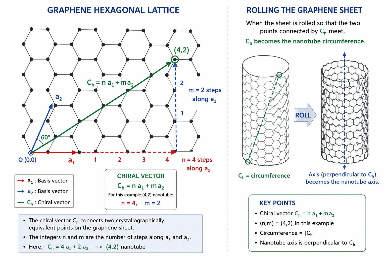
Figure 1: The graphene hexagonal lattice with basis vectors a₁ and a₂. The chiral vector Ch = n a₁ + m a₂ (shown here for a (4,2) nanotube) connects two crystallographically equivalent points on the graphene sheet. When the sheet is rolled so that these two points meet, the chiral vector becomes the nanotube circumference, and the direction perpendicular to it becomes the nanotube axis. The integers n and m are literally the number of steps along each lattice direction. | Image shows: hexagonal graphene lattice, two basis vectors a₁ and a₂ at 60°, a chiral vector drawn from origin to point (4,2), clear labeling of n=4 steps and m=2 steps, indication of rolling direction
4.3 Physical Meaning of n and m
What do these integers actually represent?
- n: The number of steps along the a₁ direction
- m: The number of steps along the a₂ direction
Think of it as giving directions on a hexagonal grid: "Go n steps in the first direction, then m steps in the second direction." The endpoint of this journey defines where the graphene sheet connects to itself to form a closed cylinder.
For example:
- (5,5) means 5 steps along a₁ and 5 steps along a₂
- (10,0) means 10 steps along a₁ and 0 steps along a₂
- (8,4) means 8 steps along a₁ and 4 steps along a₂
4.4 Nanotube Diameter from (n,m)
The chiral vector length |Ch| equals the circumference of the nanotube. Therefore, the nanotube diameter dt is:
where a = 0.246 nm is the graphene lattice constant.
dt = (0.246 nm / π) × √(10² + 10×10 + 10²) = (0.0783 nm) × √300 = 1.36 nm
5. Types of Carbon Nanotubes Based on Chirality
Not all combinations of (n,m) are equally important. In fact, the relationship between n and m defines three fundamental types of carbon nanotubes, each with distinct structural symmetry and electronic properties.
5.1 Armchair Carbon Nanotubes (n = m)
Definition: When the two chiral indices are equal (n = m), the resulting nanotube is called an armchair nanotube.
Examples: (5,5), (10,10), (15,15)
Why "armchair"? If you look at the nanotube along its axis, the arrangement of hexagons at the edge forms a pattern resembling the arms of an armchair.
Key Properties of Armchair CNTs:
- Electronic Behavior: Always metallic (zero band gap)
- Chiral Angle: θ = 30°
- Symmetry: Highest degree of mirror symmetry
- Electronic Structure: Electron states cross the Fermi level, allowing conduction
Why armchair CNTs are always metallic: In these structures, the periodic boundary conditions around the circumference align perfectly with the graphene's electronic structure in such a way that there is always a conduction path at the Fermi energy. This is a direct consequence of the zone-folding approximation in solid-state physics.
5.2 Zigzag Carbon Nanotubes (m = 0)
Definition: When m = 0, the nanotube is called a zigzag nanotube.
Examples: (10,0), (15,0), (20,0)
Why "zigzag"? Looking along the tube axis, the carbon-carbon bonds at the edge form a zigzag pattern.
Key Properties of Zigzag CNTs:
- Electronic Behavior: Can be metallic OR semiconducting, depending on n
- Chiral Angle: θ = 0°
- Metallic Condition: n is divisible by 3 → metallic; otherwise → semiconducting
- Examples: (9,0), (12,0), (15,0) are metallic; (10,0), (11,0), (13,0) are semiconducting
Important note: Unlike armchair nanotubes which are always metallic, zigzag nanotubes require checking whether n is a multiple of 3 to determine their conductivity. This is a direct consequence of the general metallic/semiconducting rule we will discuss in Section 9.
5.3 Chiral Carbon Nanotubes (n ≠ m, m ≠ 0)
Definition: When n ≠ m and m ≠ 0, the nanotube is called a chiral nanotube. (Note: the word "chiral" here refers to the specific type, even though all nanotubes have chirality as a general property.)
Examples: (10,5), (12,8), (15,3)
Key Properties of Chiral CNTs:
- Electronic Behavior: Mostly semiconducting (with rare metallic exceptions)
- Chiral Angle: 0° < θ < 30° (intermediate value)
- Structural Feature: Helical arrangement of hexagons around the tube
- Optical Activity: Can exhibit circular dichroism due to helical structure
- Handedness: Come in left-handed and right-handed forms (true chirality in the chemical sense)
Chiral nanotubes are the most common type synthesized in laboratories, but they are also the most challenging to characterize and separate because each (n,m) combination has unique properties.
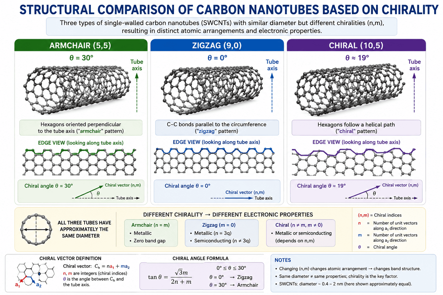
Figure 2: Structural comparison of the three types of carbon nanotubes based on chirality. Left: Armchair (5,5) showing the characteristic "armchair" edge pattern when viewed along the tube axis, with carbon hexagons oriented perpendicular to the axis (θ = 30°). Center: Zigzag (9,0) showing the "zigzag" edge pattern with carbon-carbon bonds parallel to the circumference (θ = 0°). Right: Chiral (10,5) showing the helical twist of the hexagonal pattern around the tube (θ ≈ 19°). All three structures have approximately the same diameter but completely different electronic properties due to their different chiralities. | Image shows: three side-by-side nanotube structures, clear hexagonal lattice patterns, edge views showing armchair vs zigzag patterns, chiral angle θ indicated, color-coding or labels for (n,m) indices, arrows indicating tube axis direction
6. Chiral Angle: From 0° to 30°
The chiral angle θ is the angle between the chiral vector Ch and the zigzag direction (the a₁ direction) in the graphene lattice.
6.1 Mathematical Definition
This formula gives the chiral angle for any (n,m) nanotube.
6.2 Range and Interpretation
Due to the hexagonal symmetry of graphene, the chiral angle is always between 0° and 30°:
- θ = 0° → Zigzag nanotube (m = 0)
- θ = 30° → Armchair nanotube (n = m)
- 0° < θ < 30° → Chiral nanotube
6.3 Example Calculations
Example 1: (10,0) zigzag nanotube
Example 2: (10,10) armchair nanotube
Example 3: (12,6) chiral nanotube
7. Why Chirality is Critically Important
At this point, you might be wondering: why does this geometric property matter so much? The answer lies in how chirality controls virtually every significant physical property of carbon nanotubes.
7.1 Electronic Conductivity
As we've already seen, chirality determines whether a CNT is metallic (conducts like copper wire) or semiconducting (conducts only under certain conditions). This is not a small difference — it's the difference between using the nanotube in a wire versus using it in a transistor.
7.2 Optical Properties
The optical absorption and emission spectra of CNTs are strongly chirality-dependent. Each (n,m) nanotube absorbs and emits light at specific wavelengths determined by its electronic band structure. This property is used for:
- Chirality identification through photoluminescence spectroscopy
- Optical sensors that change color based on molecular binding
- Biological imaging using CNT fluorescence
7.3 Mechanical Properties
The mechanical strength and elasticity show some chirality dependence, though less dramatic than electronic properties. Armchair nanotubes tend to have slightly higher tensile strength than zigzag nanotubes of the same diameter.
7.4 Thermal Transport
Thermal conductivity in CNTs is also chirality-dependent, with metallic nanotubes generally showing higher thermal conductivity than semiconducting ones due to the additional electronic contribution to heat transport.
7.5 Chemical Reactivity
The curvature-induced strain and electronic structure variations make different chiralities react differently with chemical species, affecting functionalization and sensing applications.
8. Electronic Band Structure and Conductivity
To understand why chirality controls conductivity, we need to briefly explore the electronic band structure of carbon nanotubes.
8.1 Origin from Graphene Band Structure
Graphene has a unique electronic structure: it is a zero-band-gap semiconductor (or "semimetal"). The valence and conduction bands touch at six points in momentum space called the K and K' points (or Dirac points). At these points, electrons behave as if they have zero effective mass and travel at constant velocity.
8.2 Quantum Confinement in Nanotubes
When graphene is rolled into a nanotube, electrons are confined in the circumferential direction but remain free to move along the tube axis. This creates one-dimensional quantum confinement.
The circumferential confinement imposes a periodic boundary condition:
This equation means that only certain electron momenta are allowed around the tube circumference. The allowed states form discrete "subbands" in the electronic structure.
8.3 Metallic vs Semiconducting Behavior
Whether the nanotube is metallic or semiconducting depends on whether any of these allowed subbands pass through the graphene K points (the Dirac points where the conduction and valence bands touch).
If YES → The nanotube is metallic (zero band gap)
If NO → The nanotube is semiconducting (finite band gap)
8.4 Density of States
The density of electronic states in a 1D system shows characteristic spikes called Van Hove singularities. These appear as sharp peaks in optical absorption spectra and are used to identify CNT chirality experimentally.
Metallic nanotubes have a finite density of states at the Fermi level, while semiconducting nanotubes have a gap in the density of states.
9. The Metallic vs Semiconducting Rule
Now we arrive at one of the most important predictive rules in carbon nanotube science.
This rule can be written mathematically as:
Otherwise → SEMICONDUCTING
9.1 Why This Rule Works
This simple rule emerges from the mathematical analysis of which quantum states intersect the graphene K points. The condition (n − m) = 3q is exactly the requirement for at least one allowed circumferential momentum state to pass through a K point.
9.2 Applying the Rule: Examples
Example 1: (10,10) armchair
Example 2: (12,0) zigzag
Example 3: (10,0) zigzag
Example 4: (12,8) chiral
Example 5: (15,3) chiral
9.3 Statistical Distribution
According to this rule, approximately 1/3 of all possible CNTs are metallic and 2/3 are semiconducting. This is because among any three consecutive values of (n−m), exactly one will be divisible by 3.
However, all armchair nanotubes (n = m) are metallic because n − m = 0, which is always divisible by 3.
9.4 Band Gap of Semiconducting CNTs
For semiconducting nanotubes, the band gap Eg is inversely proportional to the diameter:
where dt is the nanotube diameter in nanometers.
This means smaller-diameter semiconducting nanotubes have larger band gaps, which is a consequence of stronger quantum confinement.
10. Experimental Determination of Chirality
In the laboratory, how do we actually measure the chirality of a carbon nanotube? Several techniques have been developed:
10.1 Raman Spectroscopy
Principle: Raman spectroscopy measures the vibrational modes of carbon-carbon bonds. The frequencies and intensities of specific Raman peaks (particularly the radial breathing mode and the G-band) are chirality-dependent.
Radial Breathing Mode (RBM): The RBM frequency is inversely proportional to the nanotube diameter:
where A ≈ 248 cm⁻¹·nm and B ≈ 0 for individual nanotubes.
Advantages: Fast, non-destructive, can be performed on single nanotubes
Limitations: Requires calibration curves; cannot uniquely identify all (n,m) values without additional information
10.2 Photoluminescence Spectroscopy
Principle: Semiconducting CNTs emit light when optically excited. The excitation and emission wavelengths depend on the band structure, which is determined by (n,m).
Method: Create a 2D map plotting excitation wavelength vs emission wavelength. Each (n,m) semiconducting nanotube appears as a distinct peak in this map.
Advantages: Can uniquely identify many semiconducting chiralities; works in solution
Limitations: Only works for semiconducting CNTs; metallic CNTs do not fluoresce
10.3 Electron Diffraction (TEM)
Principle: Transmission electron microscopy with electron diffraction can directly image the nanotube structure and measure the chiral angle from the diffraction pattern.
Advantages: Direct structural measurement; works for all CNT types
Limitations: Requires sophisticated equipment; potential beam damage; low throughput
10.4 Scanning Tunneling Microscopy (STM)
Principle: STM can directly image the atomic structure of the nanotube surface, revealing the hexagonal pattern orientation and allowing direct determination of (n,m).
Advantages: Atomic-scale direct imaging; definitive chirality assignment
Limitations: Requires flat substrates; complex sample preparation; very low throughput
10.5 Optical Absorption Spectroscopy
Principle: CNTs show characteristic absorption peaks corresponding to transitions between Van Hove singularities. The peak positions are chirality-specific.
Advantages: Works on bulk samples; relatively simple instrumentation
Limitations: Peak overlap in mixtures; requires spectral deconvolution for accurate assignment
11. Chirality-Controlled Synthesis
One of the greatest challenges in carbon nanotube research is synthesizing nanotubes with a specific, predetermined chirality. Standard synthesis methods — chemical vapor deposition (CVD), arc discharge, and laser ablation — produce mixtures of many different chiralities.
11.1 The Chirality Control Challenge
Why is chirality control so difficult? During CNT growth, the nanotube cap nucleates on a catalyst particle. The cap structure determines the subsequent chirality. However, many different cap structures are energetically similar, leading to a statistical distribution of chiralities in the product.
11.2 Strategies for Chirality Control
Catalyst Engineering: Designing catalyst nanoparticles with specific crystal facets that template particular chiralities. Some success has been achieved with Co-Mo catalysts selectively growing specific semiconducting chiralities.
Growth Condition Optimization: Controlling temperature, carbon feedstock, and gas composition to favor certain chiralities. For example, lower temperatures tend to favor smaller-diameter nanotubes.
Cloning Approach: Using existing CNT segments as templates to grow additional nanotubes of the same chirality (epitaxial growth).
DNA-Assisted Growth: Using DNA sequences that selectively bind to and stabilize specific chiralities during synthesis.
11.3 Post-Synthesis Separation
Since chirality-selective synthesis remains challenging, post-synthesis separation is often used:
- Density Gradient Ultracentrifugation (DGU): CNTs are coated with surfactants and separated by density in a centrifuge. Different chiralities have slightly different buoyant densities.
- Gel Chromatography: CNTs are separated based on their interactions with a gel column. Metallic and semiconducting CNTs can be separated, and sometimes individual chiralities.
- Selective Chemistry: Exploiting the fact that metallic CNTs are more reactive than semiconducting ones. Metallic CNTs can be selectively functionalized and then removed or destroyed.
- Electrical Breakdown: Applying high current preferentially burns out metallic CNTs in a device, leaving only semiconducting ones.
12. Applications of Chirality in Technology
The ability to control and exploit CNT chirality enables transformative applications across multiple fields.
12.1 Nanoelectronics
CNT Field-Effect Transistors (CNTFETs): Semiconducting CNTs are used as the channel material in transistors. The band gap, controlled by chirality, determines the on/off ratio and switching characteristics. Specific chiralities like (19,0) or (10,9) are targeted for optimal device performance.
Interconnects: Metallic armchair CNTs can carry current densities >10⁹ A/cm², far exceeding copper. They are being explored as nanoscale wires in integrated circuits.
12.2 Sensors
Chemical Sensors: The electrical conductivity of semiconducting CNTs changes when molecules adsorb on the surface. Different chiralities have different sensitivities to specific molecules, enabling "chirality-coded" sensor arrays.
Biosensors: DNA-wrapped CNTs with specific chiralities can detect biomarkers, glucose, or specific proteins through fluorescence changes.
12.3 Optoelectronics
Light-Emitting Devices: Electrically pumped CNT LEDs can emit at specific wavelengths determined by chirality, enabling color-tunable light sources.
Photodetectors: Semiconducting CNTs absorb light at chirality-specific wavelengths, making them useful for wavelength-selective photodetection in the near-infrared.
12.4 Energy Storage and Conversion
Lithium-Ion Batteries: Metallic CNTs provide high electrical conductivity in electrodes, while semiconducting CNTs can participate in redox reactions. Chirality affects both performance and cycle life.
Solar Cells: CNT thin films with controlled chirality distributions are used as transparent electrodes and active layers in photovoltaics.
12.5 Quantum Devices
Quantum Computing: CNT quantum dots, where chirality controls the energy level spacing, are being explored as qubits.
Single-Photon Sources: Specific defects in semiconducting CNTs can emit single photons on demand, useful for quantum communication.
12.6 Composite Materials
Structural Composites: Adding small amounts of metallic CNTs to polymers creates electrically conductive composites for EMI shielding and static dissipation.
Thermal Management: High-thermal-conductivity metallic CNTs in composites improve heat dissipation in electronics.
13. Comparison Table: Armchair vs Zigzag vs Chiral
Here is a comprehensive comparison of the three CNT types based on their chirality characteristics:
| Property | Armchair (n = m) | Zigzag (m = 0) | Chiral (n ≠ m, m ≠ 0) |
|---|---|---|---|
| Chiral Indices | (n, n) | (n, 0) | (n, m) with n ≠ m, m ≠ 0 |
| Chiral Angle | θ = 30° | θ = 0° | 0° < θ < 30° |
| Electrical Behavior | Always metallic | Metallic if n = 3q; semiconducting otherwise | Mostly semiconducting (metallic if n−m = 3q) |
| Examples | (5,5), (10,10), (15,15) | (10,0), (12,0), (15,0) | (10,5), (12,8), (15,3) |
| Structural Symmetry | Highest mirror symmetry | Mirror symmetry plane perpendicular to axis | Helical structure; no mirror plane |
| Handedness (Enantiomers) | No handedness (achiral) | No handedness (achiral) | Left-handed and right-handed forms exist |
| Optical Activity | No circular dichroism | No circular dichroism | Can show circular dichroism |
| Synthesis Frequency | Relatively rare in random synthesis | Relatively rare in random synthesis | Most common (vast majority of CNTs) |
| Band Gap (if semiconducting) | N/A (always metallic) | Eg ≈ 0.8/dt eV | Eg ≈ 0.8/dt eV |
| Applications | Interconnects, transparent conductors | Mixed metallic/semiconducting devices | Transistors, sensors, photonics |
14. Frequently Asked Questions
Q1: Is every carbon nanotube chiral?
In the general sense, yes — every CNT has a chirality (a geometric structure defined by (n,m)). However, in the specific terminology, "chiral" CNTs refer to those where n ≠ m and m ≠ 0. Armchair and zigzag CNTs are considered "achiral" types because they have mirror symmetry planes.
Q2: Why are armchair CNTs always metallic?
Armchair CNTs (n = m) are always metallic because their periodic boundary conditions force at least one of the allowed electron momentum states to pass exactly through the Dirac points (K points) of graphene's band structure, where the conduction and valence bands touch. This creates a continuous density of states at the Fermi level.
Q3: Can a zigzag CNT be metallic?
Yes! A zigzag CNT (n,0) is metallic if n is divisible by 3. For example, (9,0), (12,0), and (15,0) are metallic, while (10,0), (11,0), and (13,0) are semiconducting. This follows from the general rule (n−m) = 3q for metallicity.
Q4: What determines CNT chirality during synthesis?
Chirality is primarily determined by the initial cap structure that forms on the catalyst particle during nucleation. The cap's geometric structure (number of pentagons, hexagons, and their arrangement) dictates the subsequent chirality. Factors influencing cap formation include catalyst particle size, crystal structure, temperature, carbon feedstock, and growth kinetics.
Q5: How does chirality affect the band gap?
Chirality determines whether a CNT is metallic (zero band gap) or semiconducting (finite band gap) through the (n−m) = 3q rule. For semiconducting CNTs, the band gap is inversely proportional to diameter: Eg ≈ 0.8 eV·nm / dt. Different chiralities with the same diameter can have different band gaps due to variations in quantum confinement details.
Q6: What is the difference between chirality and helicity?
Chirality refers to the overall geometric structure defined by (n,m) indices. Helicity specifically refers to the helical twist angle of the hexagonal lattice around the tube axis. All chiral-type CNTs (n ≠ m, m ≠ 0) have helicity and come in left-handed and right-handed forms. Armchair and zigzag CNTs have zero helicity (straight lattice lines along the tube).
Q7: Why is chirality control so difficult during synthesis?
Several factors make chirality control challenging: (1) Many different cap structures (and thus chiralities) have similar formation energies, (2) the catalyst-CNT interface is dynamic and complex, (3) growth conditions affect all chiralities simultaneously, (4) thermodynamic factors compete with kinetic factors, and (5) defect formation can change chirality during growth. Despite progress, no method yet achieves >95% single-chirality synthesis for arbitrary (n,m) targets.
Q8: Can chirality change during CNT processing?
Chirality is generally stable under normal processing conditions. However, extreme conditions — high-energy electron beams, intense laser irradiation, or chemical etching creating large defects — can alter or destroy the structure. Stone-Wales defects (bond rotation) do not change chirality but can locally modify electronic properties.
15. Worked Examples
Example 1: Determine all properties of a (9,6) CNT
Given: (n,m) = (9,6)
Find: Type, chiral angle, diameter, electronic behavior
Solution:
Step 1: Determine type
Since n ≠ m (9 ≠ 6) and m ≠ 0, this is a chiral-type CNT.
Step 2: Calculate chiral angle
θ = tan⁻¹ [ (√3 × 6) / (2×9 + 6) ]
θ = tan⁻¹ [ 10.39 / 24 ]
θ = tan⁻¹(0.433) = 23.4°
Step 3: Calculate diameter
dt = (0.246 nm / π) × √(81 + 54 + 36)
dt = 0.0783 nm × √171
dt = 0.0783 nm × 13.08 = 1.02 nm
Step 4: Determine electronic behavior
Since (n−m) is divisible by 3, this CNT is METALLIC.
Summary: (9,6) is a metallic, chiral-type CNT with θ = 23.4° and diameter 1.02 nm.
Example 2: Band gap calculation for a semiconducting CNT
Given: A (10,5) carbon nanotube
Find: Electronic type and band gap
Solution:
Step 1: Check if metallic or semiconducting
5 is not divisible by 3, so this CNT is SEMICONDUCTING.
Step 2: Calculate diameter
dt = 0.0783 nm × √(100 + 50 + 25)
dt = 0.0783 nm × √175
dt = 0.0783 nm × 13.23 = 1.04 nm
Step 3: Calculate band gap
Eg = 0.8 eV·nm / 1.04 nm = 0.77 eV
Interpretation: This band gap of 0.77 eV is in the near-infrared energy range (photon wavelength ≈ 1600 nm), making this CNT useful for NIR photodetectors and telecommunications applications.
Example 3: Predicting properties from diameter and type
Given: A zigzag CNT with diameter 0.78 nm
Find: Possible (n,m) values and electronic behavior
Solution:
Step 1: For zigzag CNTs, m = 0, so (n,0). The diameter formula simplifies:
0.78 nm = (0.246 nm / π) × n
n = 0.78 nm × π / 0.246 nm = 9.96 ≈ 10
Step 2: The CNT is (10,0).
Step 3: Electronic behavior:
10 is not divisible by 3, so (10,0) is SEMICONDUCTING.
Step 4: Band gap:
Conclusion: A 0.78 nm diameter zigzag CNT is (10,0), semiconducting with a band gap of approximately 1.03 eV.
16. Key Takeaways
Essential Concepts: Chirality of Carbon Nanotubes
1. CHIRALITY DEFINITION: Chirality is the geometric "twist" or wrapping angle of the graphene lattice when rolled into a cylindrical nanotube. It is completely specified by two integers (n,m) called chiral indices.
2. CHIRAL VECTOR: The mathematical description is Ch = n a₁ + m a₂, where a₁ and a₂ are the graphene lattice vectors. This vector becomes the nanotube circumference.
3. THREE TYPES: Based on (n,m), CNTs fall into three categories:
• Armchair (n = m): Always metallic, θ = 30°
• Zigzag (m = 0): Metallic if n = 3q, θ = 0°
• Chiral (n ≠ m, m ≠ 0): Mostly semiconducting, 0° < θ < 30°
4. METALLIC/SEMICONDUCTING RULE: If (n − m) is divisible by 3 → metallic; otherwise → semiconducting. This simple rule predicts electrical behavior from geometry alone.
5. DIAMETER FORMULA: dt = (a/π) × √(n² + nm + m²), where a = 0.246 nm is the graphene lattice constant.
6. CHIRAL ANGLE: θ = tan⁻¹[(√3 m)/(2n + m)], always between 0° and 30° due to hexagonal symmetry.
7. BAND GAP: For semiconducting CNTs, Eg ≈ 0.8 eV·nm / dt. Smaller diameter = larger band gap.
8. WHY IT MATTERS: Chirality controls electronic conductivity, optical absorption/emission, chemical reactivity, thermal transport, and mechanical properties. It's the primary design parameter for CNT applications.
9. CHARACTERIZATION: Experimental methods include Raman spectroscopy (RBM mode), photoluminescence mapping, electron diffraction, STM imaging, and optical absorption.
10. SYNTHESIS CHALLENGE: Achieving single-chirality synthesis remains one of the grand challenges. Current approaches use catalyst engineering, growth optimization, or post-synthesis separation.
11. APPLICATIONS: Metallic CNTs for interconnects and transparent electrodes; semiconducting CNTs for transistors, sensors, photodetectors, and photonics; chirality-specific uses in quantum devices.
12. QUANTUM ORIGIN: The metallic/semiconducting behavior arises from one-dimensional quantum confinement and whether allowed electron states intersect graphene's K points (Dirac points).
17. References
All references follow IEEE citation style. All sources are peer-reviewed journals, authoritative textbooks, or recognized academic databases.
- R. Saito, G. Dresselhaus, and M. S. Dresselhaus, Physical Properties of Carbon Nanotubes. London, UK: Imperial College Press, 1998. — The definitive textbook on CNT physics, including comprehensive treatment of chirality, electronic structure, and the zone-folding approximation.
- M. S. Dresselhaus, G. Dresselhaus, and P. Avouris, Eds., Carbon Nanotubes: Synthesis, Structure, Properties, and Applications, vol. 80. Berlin, Germany: Springer-Verlag, 2001. — Authoritative reference covering CNT structure-property relationships and the origin of chirality-dependent electronic behavior.
- J.-C. Charlier, X. Blase, and S. Roche, "Electronic and transport properties of nanotubes," Reviews of Modern Physics, vol. 79, no. 2, pp. 677–732, Apr. 2007, doi: 10.1103/RevModPhys.79.677. — Comprehensive review of electronic band structure, the metallic/semiconducting rule derivation, and transport phenomena in CNTs.
- S. Reich, C. Thomsen, and J. Maultzsch, Carbon Nanotubes: Basic Concepts and Physical Properties. Weinheim, Germany: Wiley-VCH, 2004. — Graduate-level textbook covering chiral vector mathematics, reciprocal space analysis, and experimental characterization techniques.
- A. Jorio, M. S. Dresselhaus, R. Saito, and G. Dresselhaus, Raman Spectroscopy in Graphene Related Systems. Weinheim, Germany: Wiley-VCH, 2011. — Definitive reference for using Raman spectroscopy (particularly RBM) to determine CNT chirality.
- S. M. Bachilo et al., "Structure-assigned optical spectra of single-walled carbon nanotubes," Science, vol. 298, no. 5602, pp. 2361–2366, Dec. 2002, doi: 10.1126/science.1078727. — Landmark paper establishing photoluminescence mapping for chirality assignment in semiconducting CNTs.
- H. Kataura et al., "Optical properties of single-wall carbon nanotubes," Synthetic Metals, vol. 103, no. 1–3, pp. 2555–2558, Jun. 1999, doi: 10.1016/S0379-6779(98)00278-1. — Foundational work on the relationship between CNT diameter, chirality, and optical transition energies (Kataura plot).
- J. W. G. Wildöer et al., "Electronic structure of atomically resolved carbon nanotubes," Nature, vol. 391, no. 6662, pp. 59–62, Jan. 1998, doi: 10.1038/34139. — First direct STM measurement of CNT electronic structure showing the density of states and metallic/semiconducting behavior.
- T. W. Odom, J.-L. Huang, P. Kim, and C. M. Lieber, "Atomic structure and electronic properties of single-walled carbon nanotubes," Nature, vol. 391, no. 6662, pp. 62–64, Jan. 1998, doi: 10.1038/34145. — Experimental confirmation of the (n−m) mod 3 rule for metallicity using STM.
- F. Yang et al., "Chirality-specific growth of single-walled carbon nanotubes on solid alloy catalysts," Nature, vol. 510, no. 7506, pp. 522–524, Jun. 2014, doi: 10.1038/nature13434. — Breakthrough in chirality-controlled synthesis using tungsten-based catalysts.
- H. Liu et al., "Large-scale single-chirality separation of single-wall carbon nanotubes by simple gel chromatography," Nature Communications, vol. 2, Art. no. 309, May 2011, doi: 10.1038/ncomms1313. — Demonstration of efficient post-synthesis chirality separation.
- A. A. Green and M. C. Hersam, "Nearly single-chirality single-walled carbon nanotubes produced via orthogonal iterative density gradient ultracentrifugation," Advanced Materials, vol. 23, no. 19, pp. 2185–2190, May 2011, doi: 10.1002/adma.201100034. — Advanced separation technique achieving >99% purity for specific semiconducting chiralities.
- P. Avouris, Z. Chen, and V. Perebeinos, "Carbon-based electronics," Nature Nanotechnology, vol. 2, no. 10, pp. 605–615, Oct. 2007, doi: 10.1038/nnano.2007.300. — Review of CNT applications in nanoelectronics with emphasis on chirality requirements.
- M. J. O'Connell et al., "Band gap fluorescence from individual single-walled carbon nanotubes," Science, vol. 297, no. 5581, pp. 593–596, Jul. 2002, doi: 10.1126/science.1072631. — First observation of near-infrared fluorescence from semiconducting CNTs, enabling chirality identification.
- C. Journet et al., "Large-scale production of single-walled carbon nanotubes by the electric-arc technique," Nature, vol. 388, no. 6644, pp. 756–758, Aug. 1997, doi: 10.1038/41972. — Classic paper on arc discharge synthesis producing chirality mixtures.
- R. Saito, M. Fujita, G. Dresselhaus, and M. S. Dresselhaus, "Electronic structure of chiral graphene tubules," Applied Physics Letters, vol. 60, no. 18, pp. 2204–2206, May 1992, doi: 10.1063/1.107080. — Theoretical foundation predicting the electronic properties from chirality using zone-folding.
- N. Hamada, S. Sawada, and A. Oshiyama, "New one-dimensional conductors: Graphitic microtubules," Physical Review Letters, vol. 68, no. 10, pp. 1579–1581, Mar. 1992, doi: 10.1103/PhysRevLett.68.1579. — Early theoretical prediction of metallic and semiconducting CNTs based on helicity.
- C. L. Kane and E. J. Mele, "Size, shape, and low energy electronic structure of carbon nanotubes," Physical Review Letters, vol. 78, no. 10, pp. 1932–1935, Mar. 1997, doi: 10.1103/PhysRevLett.78.1932. — Advanced theoretical treatment of how curvature and chirality affect band structure.
- J. Kong et al., "Nanotube molecular wires as chemical sensors," Science, vol. 287, no. 5453, pp. 622–625, Jan. 2000, doi: 10.1126/science.287.5453.622. — Demonstration of CNT chemical sensors with chirality-dependent sensitivity.
- R. H. Baughman, A. A. Zakhidov, and W. A. de Heer, "Carbon nanotubes—the route toward applications," Science, vol. 297, no. 5582, pp. 787–792, Aug. 2002, doi: 10.1126/science.1060928. — Comprehensive review of CNT applications across electronics, materials, and energy.
About the Author
Dr. Rolly Verma is a materials scientist with a PhD in Applied Physics from Birla Institute of Technology, Mesra. She specializes in nanomaterials and ferroelectric materials, with research experience in carbon nanostructures, perovskite oxides, and functional ceramics. Dr. Verma has served as a Women Scientist in the Department of Physics at BIT Mesra and as Guest Faculty in the Department of Physics at Ranchi University, Jharkhand. She is the founder of AdvanceMaterialsLab.com, an educational platform dedicated to supporting students and early-career researchers in materials science and nanotechnology.
For questions, corrections, or feedback on this tutorial, please contact: advancematerialslab27@gmail.com